BUSINESS AREAS
Materials Will Be With You,
The Way To Make A Better Future.
Material for CMP process


It can solve The semiconductor wafer surface defect problem that occurs during the CMP process and since the more the manufacturing of highly intensive element. The more the homogeneity is important, its needs are emerged.
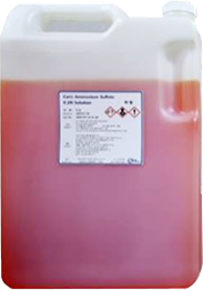
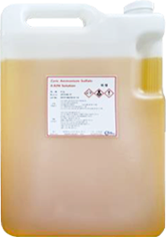
As a standard measuring solution that measures the change of concentration of H2O2, which the change with the passage of time occurs according to the external influence such as time, temperature, etc. out of the combination elements (DI water, H2O2) of slurry used as abrasive in the MP process, it maintains the homogeneity of the wafer flattening work utilizing it.


Save 50% of
the cost compared
to import products

Respond to the product
history management
and advancement of development

No domestic
manufacturing
competitor
Progress
2019.01
Completed the product registration in the semiconductor manufacturer and registered 1 NaOH-based additional radox substance
2018.06
Manufacturing patent registration [No. KR 10-1868771]
Customer

SAMSUNG

SK-hynix